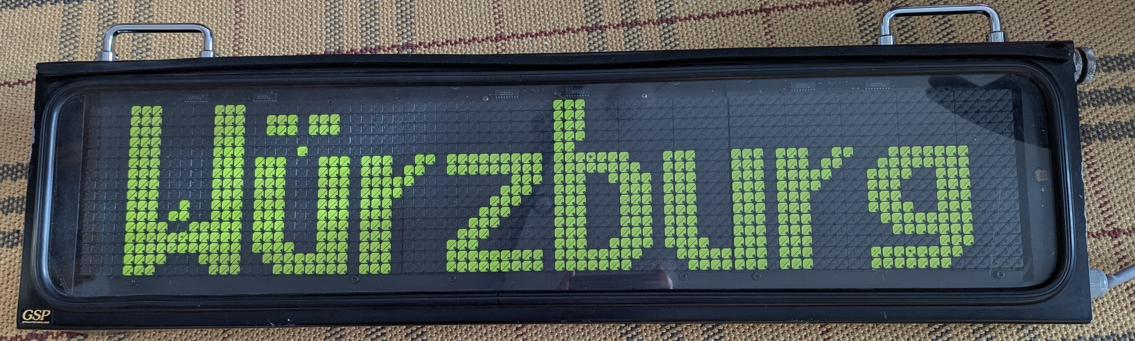
This page is part of a series on Annax flipdot modules. On this page, I'll give a rough overview of the components that make up the entire display unit and how they are connected to each other, as well as how the flip-dot display panels work. The other pages discuss the circuitry and the firmware in more detail.
In this article:
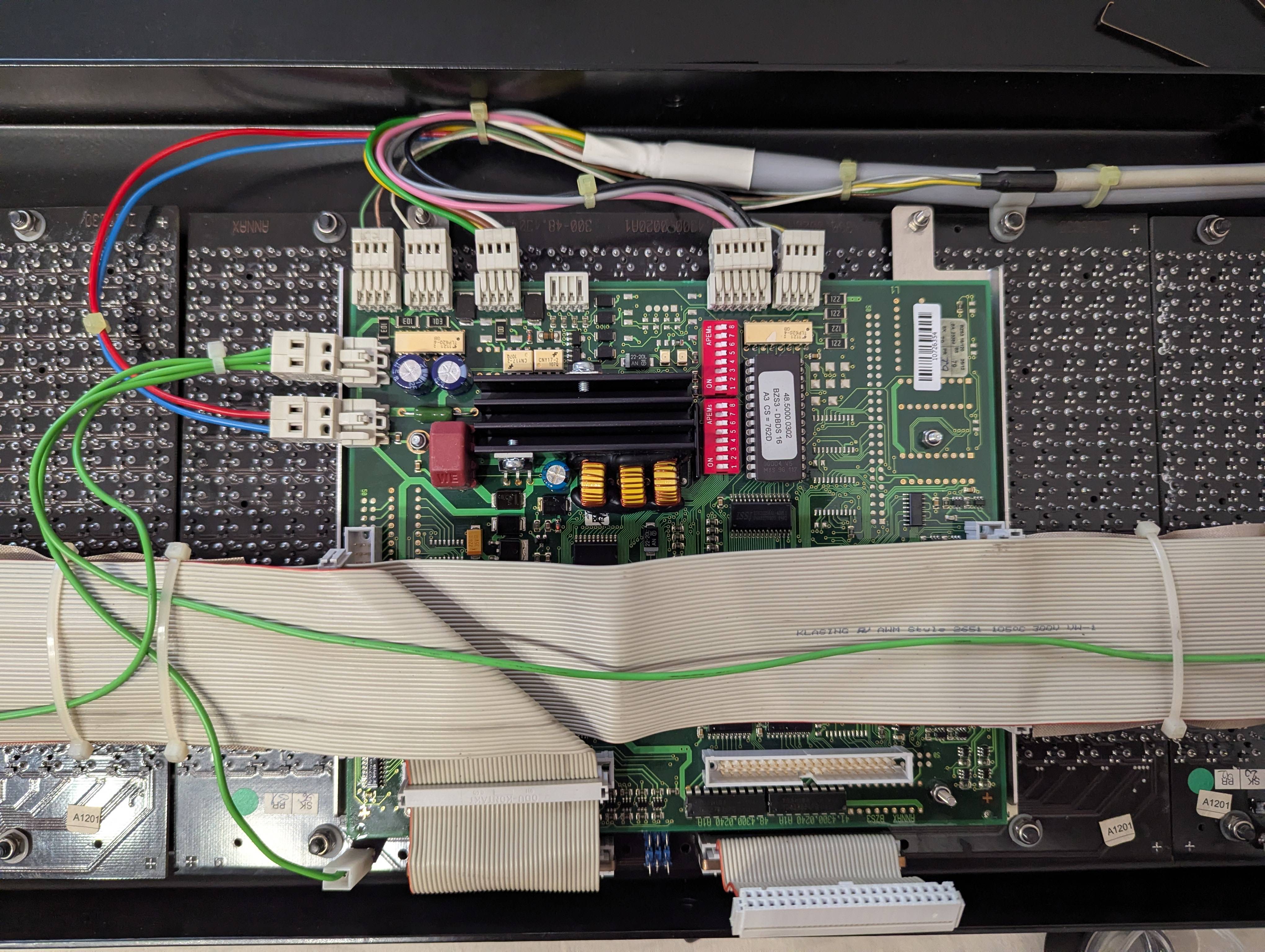
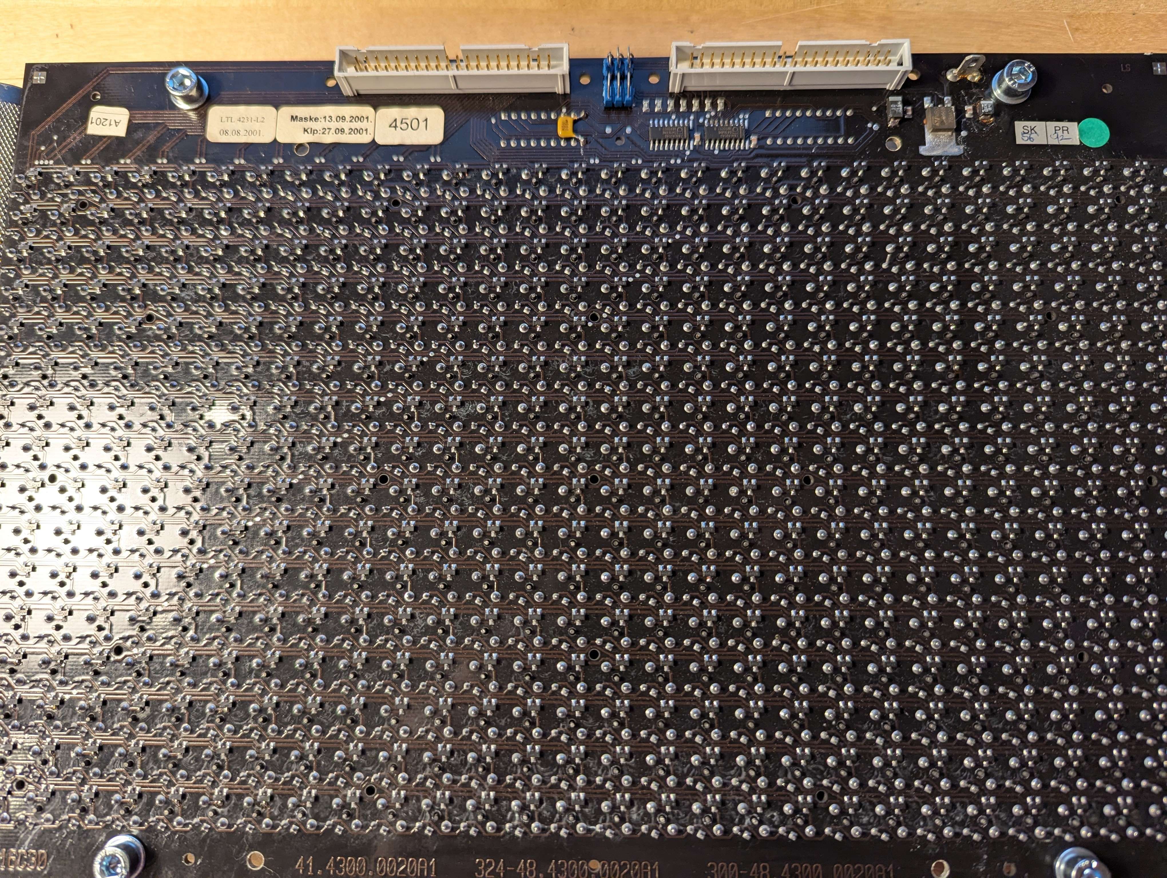
If you open the display unit, you can see the following PCBs:
A bunch of colorful wires emerge from a bundle that connects the display unit to the outside world. They carry supply voltage (likely around 26-32 volts) and connections to the train bus (IBIS/VÖV 300). A smaller, thinner bundle of wires goes to the ambient light sensor.
As you can see, the control board connects to the display panels using two 40-pin ribbon cables each, which would be more than enough to carry row and column signals for one entire panel. This suggests that there are no driver ICs on the display panels (which some other manufacturers do), but all the power switching is done on the main control board.
Additionally, we can see that more than one module is attached to some of the cables, which is a clever way to control multiple panels with comparatively few driver outputs: instead of needing (rows+columns) × (number of panels) drivers, you can e.g. use the same set of row drivers for all panels and provide each panel with separate column drivers. (The actual layout is discussed below and saves even more drivers.)
Let's remove one of the panels and figure out how it works!
(Be careful while doing so! The small magnets on the dots are quite fragile and as you can see in the topmost image on this page, I already managed to break a few pixels by hitting the leftmost panels a bit too hard on the table...)
As I said in the introduction, someone else also analyzed the same type of flipdot panel and the matrix layout (although I only found out about this after I wrote this part of the series).
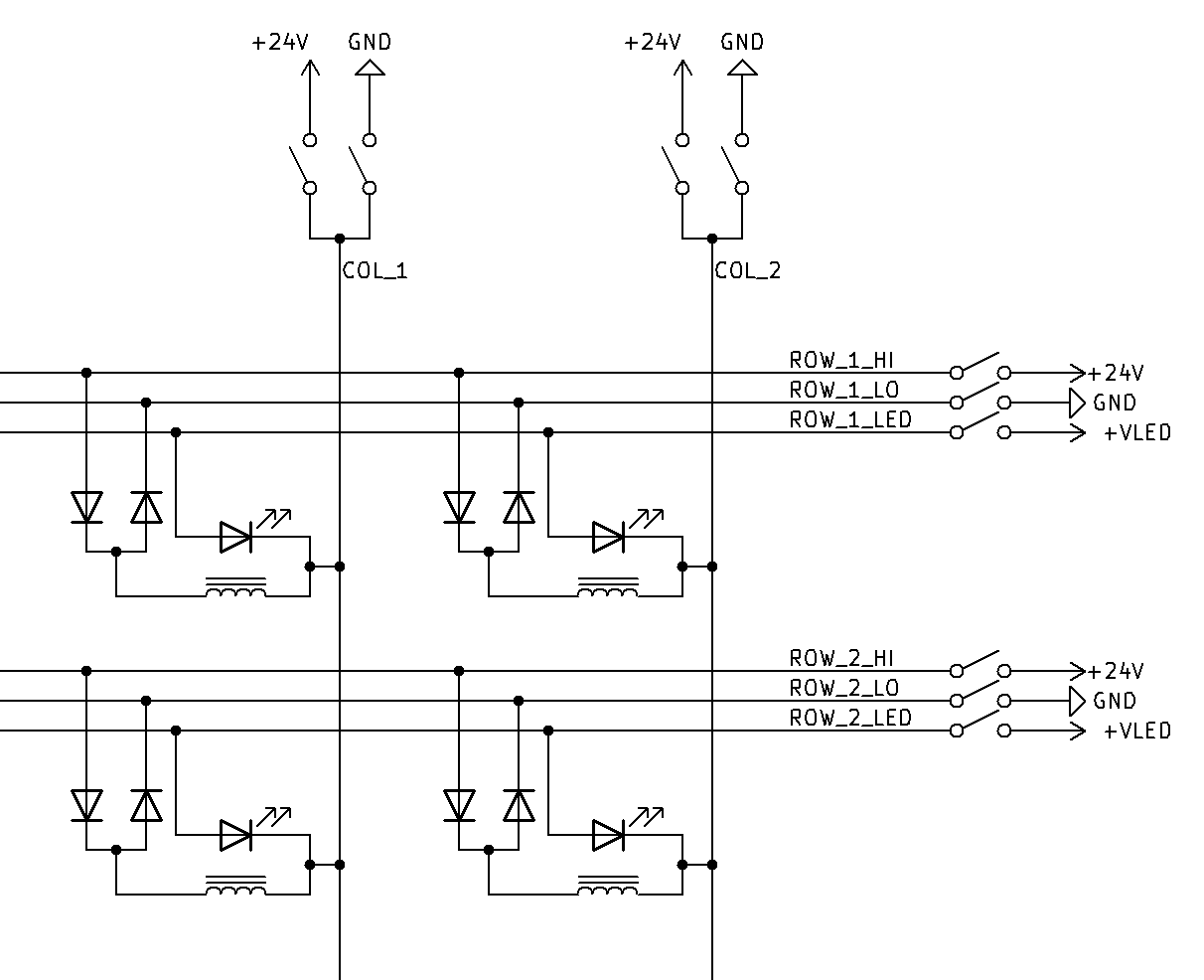
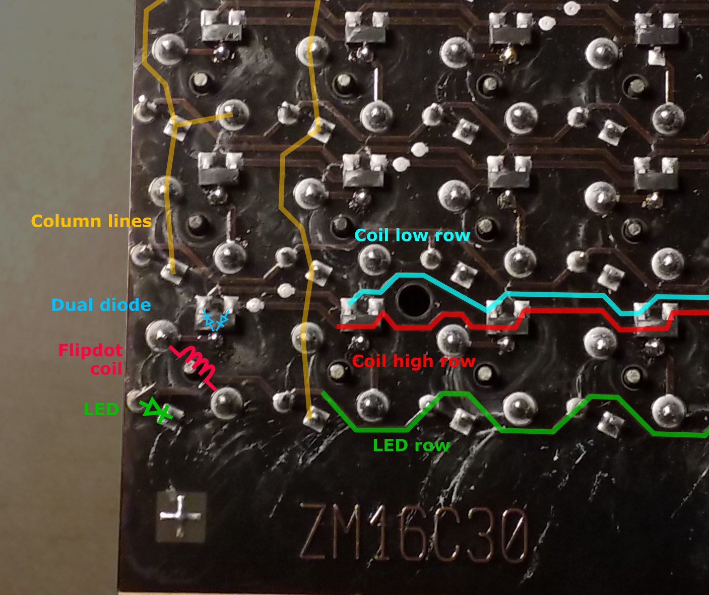
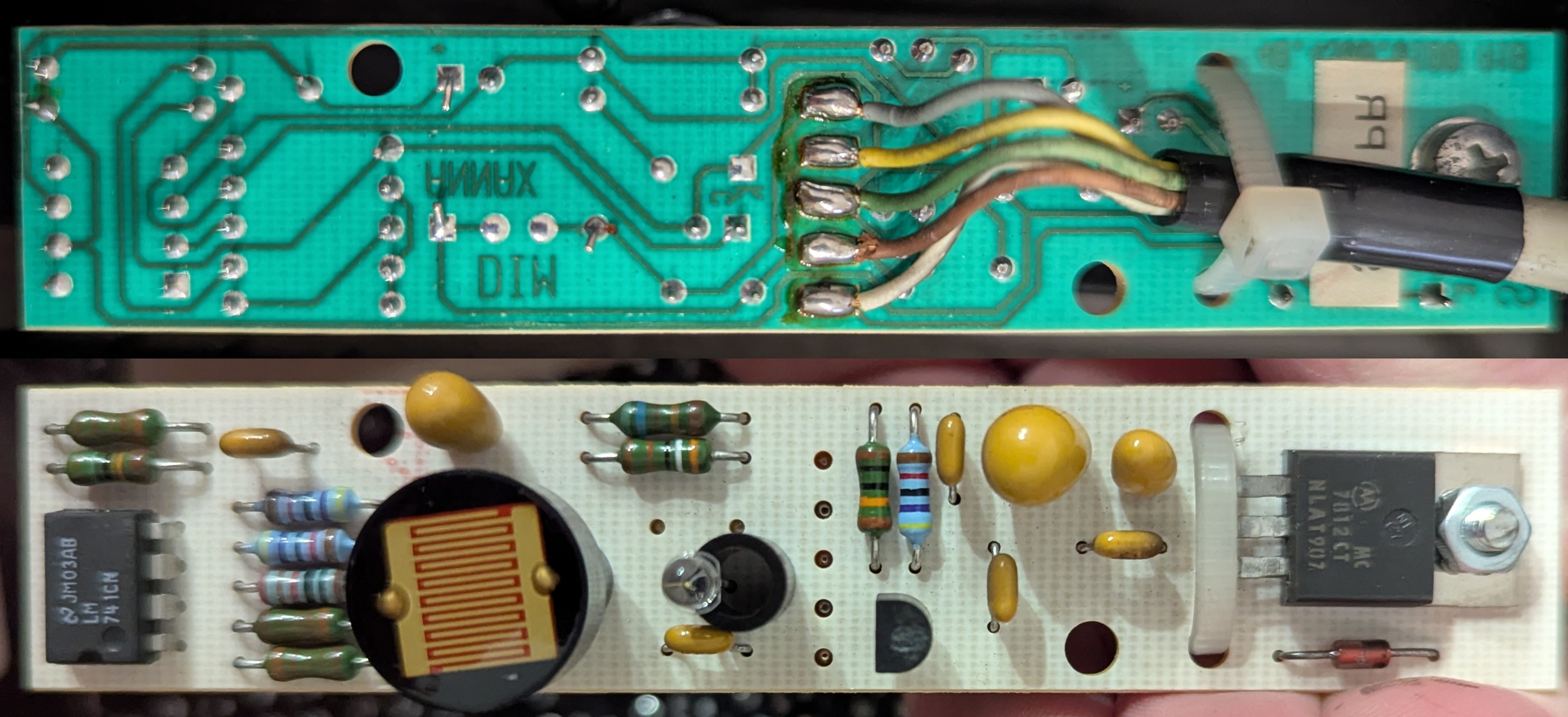
Each pixel consists of:
(If you look closely, you can see that in one pixel, the top left pin of the coil goes to the diode, while the neighboring pixel has the bottom right pixel going to the diode. I don't know a lot about magnetism, but I assume they are set up in alternating orientations to prevent neighboring pixels from interacting with each other.)
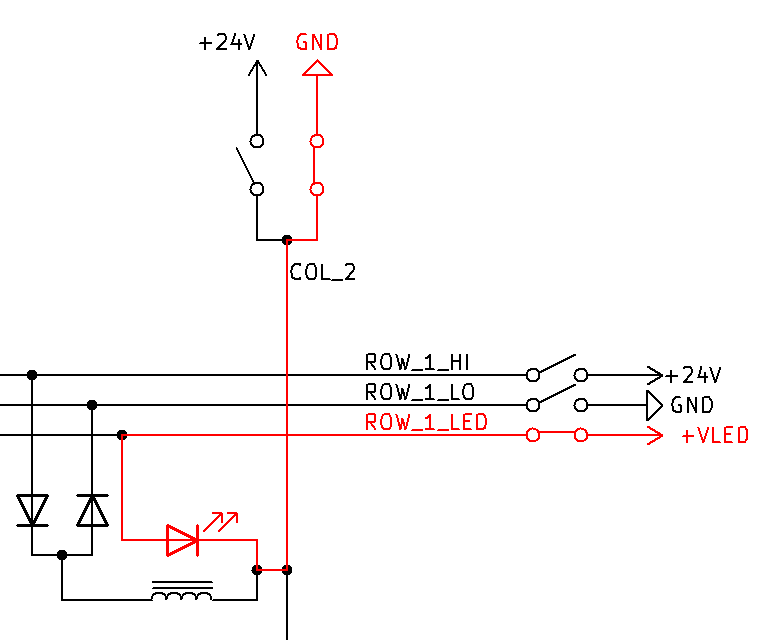
With just a single coil per pixel, the polarity of the applied voltage determines the direction a pixel is flipped: connect row to 24V and column to GND to flip it one way, connect row to GND and column to 24V to flip it the other way. Any matrix (just like a standard LED matrix) requires diodes to uniquely determine the current flow (otherwise, you would get a circuit not only through the coil you actually wanted to control, but additional paths through several coils in series). Single diodes, as in an LED matrix, however would only allow flipping pixels in a single direction.
Hence there are not one, but two coil control signals per row (coil low and coil high), and two diodes per pixel. At most one of the two signals is active at any given time. The dual diode is connected with its center pin to the coil, and the other two pins connect to the row lines (connecting the respective pins of each pixel in the same row). The other end of the coil connects to the column line (which connects all pixels in the same column). In the schematic to the right, I sketched this out for a 2 × 2 matrix.
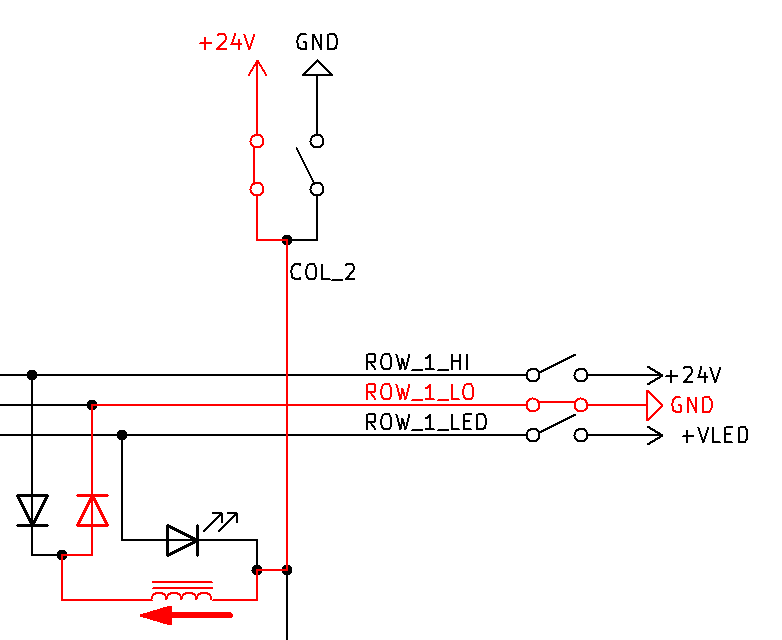
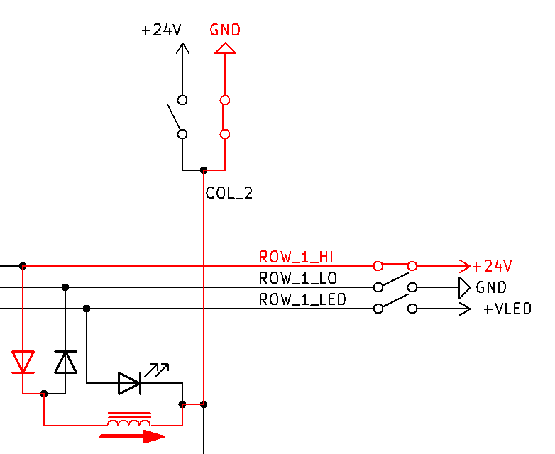
Then, to make a dot flip, you apply 24V to coil high row and GND to the column; or GND to coil low row and 24V to the column – see the left two schematics below. Since only one of the row signals is active at any given time and the other one is electrically disconnected, the other row signals (and the diode connected to it) practically "disappear" from the circuit and you're left with just one column signal, one row signal, and one diode.
To power the LEDs that are integrated in each pixel, there is a third row signal (LED row) that connects the anodes of all LEDs in the same row. The cathodes of all LEDs in the same column are connected to the same column lines that are used for the coils – see third schematic below. During flipdot switching, the LED row signals stay off and hence the LEDs are practically disconnected from the matrix during the flipping phase.
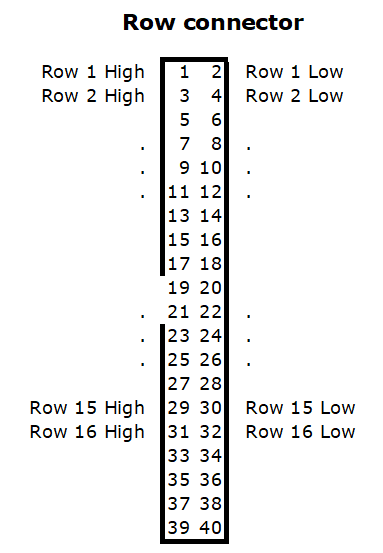
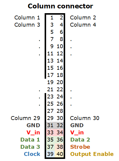
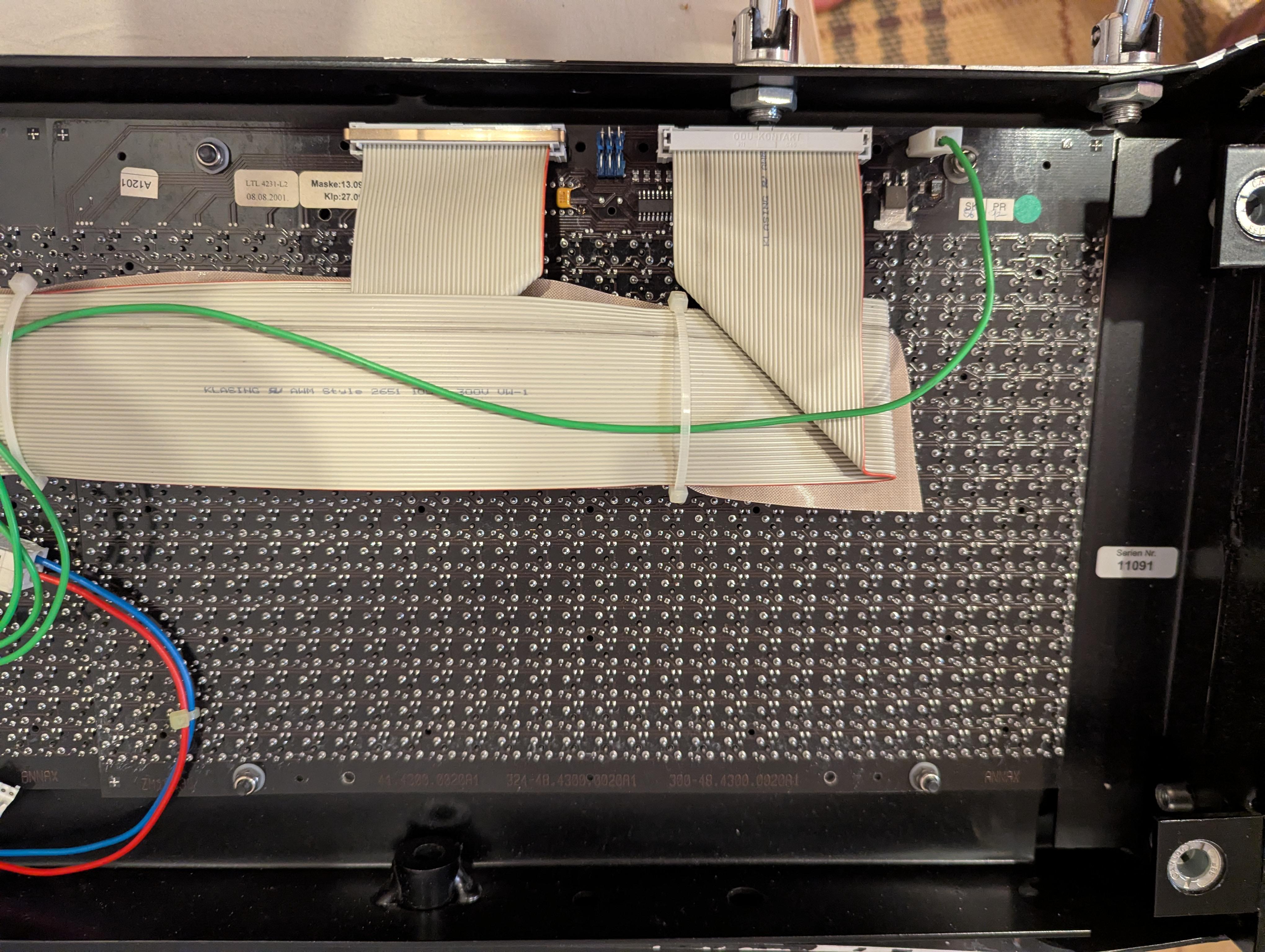
The most obvious ones are the two 40-pin IDC connectors. If you probe the signals to the matrix, you can quickly figure out how it connects to the pixels (see diagrams for pin 1 location):
There are some additional components: three jumpers (one of which is set), a 5 volt regulator, two 8-bit shift registers (74HC4094) and two 8-channel high side switches (TD62783, on the other side of the board). These are unrelated to the coils. Instead, they connect the LED row lines to the LED supply voltage, which is provided via the blade terminal (which is where the green wires mentioned earlier are plugged into).
It is quite likely that this display unit (with flipdot and LED combined) is the successor to an older model that did not include LEDs, and hence only required the two flat cables. Instead of changing the layout to include a third cable for the LEDs and including the LED drivers on the main control board, the drivers were placed on the panels themselves, requiring only a power supply wire and a small number of data lines that were placed in the unused part of the column connector. This also explains the jumpers: the panel needs to know which LED signals (panel 1/2/3) it should respond to. For the flipdot coils, no such configuration jumpers are necessary since the control board has two separate connectors for those anyway, so only the panel at the "intersection" (see also mapping of connectors to panels a couple paragraphs below) will actually flip.
This gives us the following pinout for the column connector:
Using that pinout, you could build your own control board – you need a bunch of driver ICs that can switch 24V to coil high row, GND to coil low row, and either 24V or GND to the column lines; as well as controlling the shift register if the LEDs shall be activated as well.
In the short video below, you can see a single dot flip, by manually providing a short (1-5 ms) pulse on the corresponding pins. Flipdot coils typically require pulses around 1 to 5 milliseconds. Continuously providing the coil with current will likely cause it to burn pretty quickly (Or maybe not, but these displays have become rare enough by now that I really don't want to try...). I used an ATtiny on a breadboard to generate such short pulses.
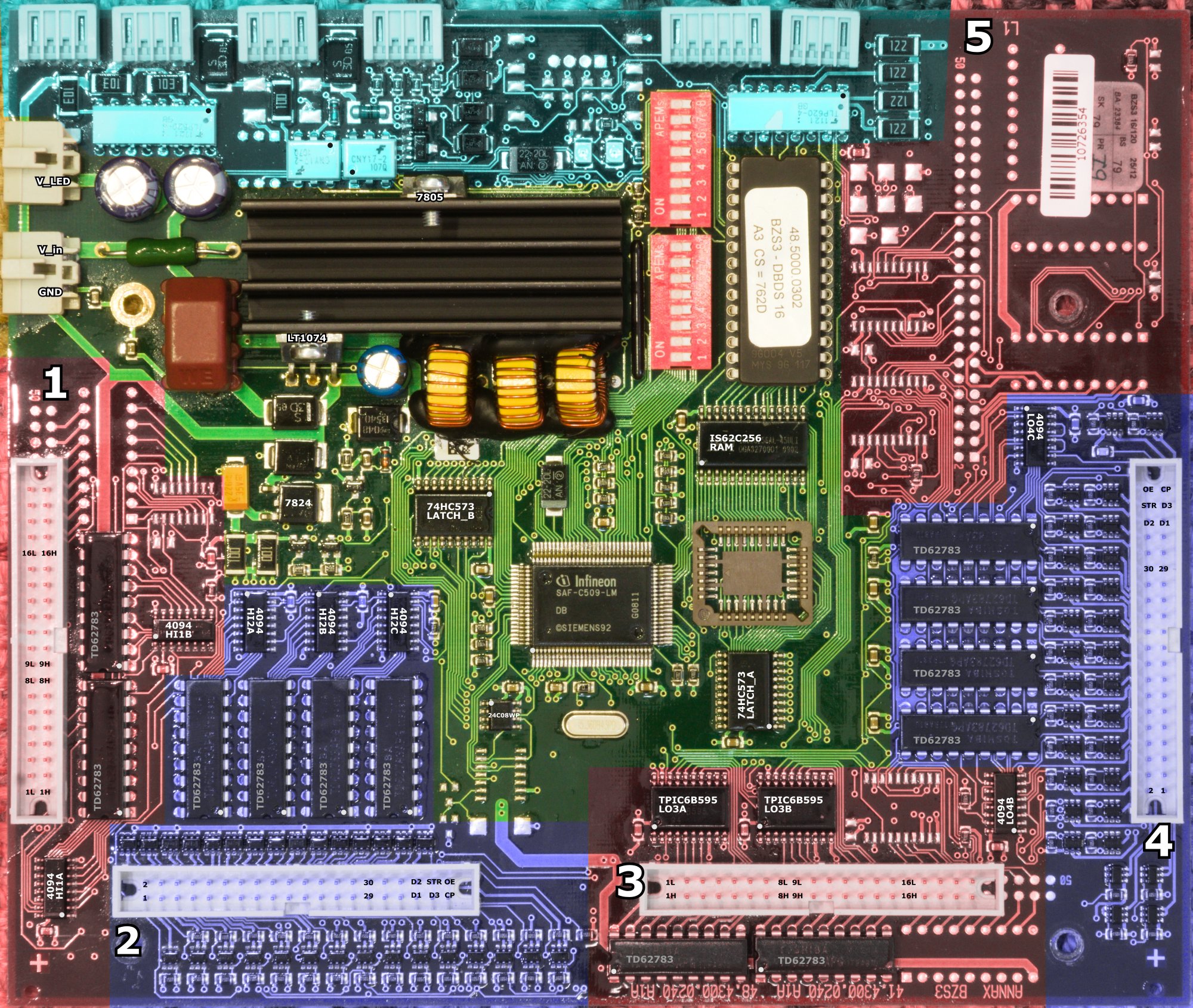
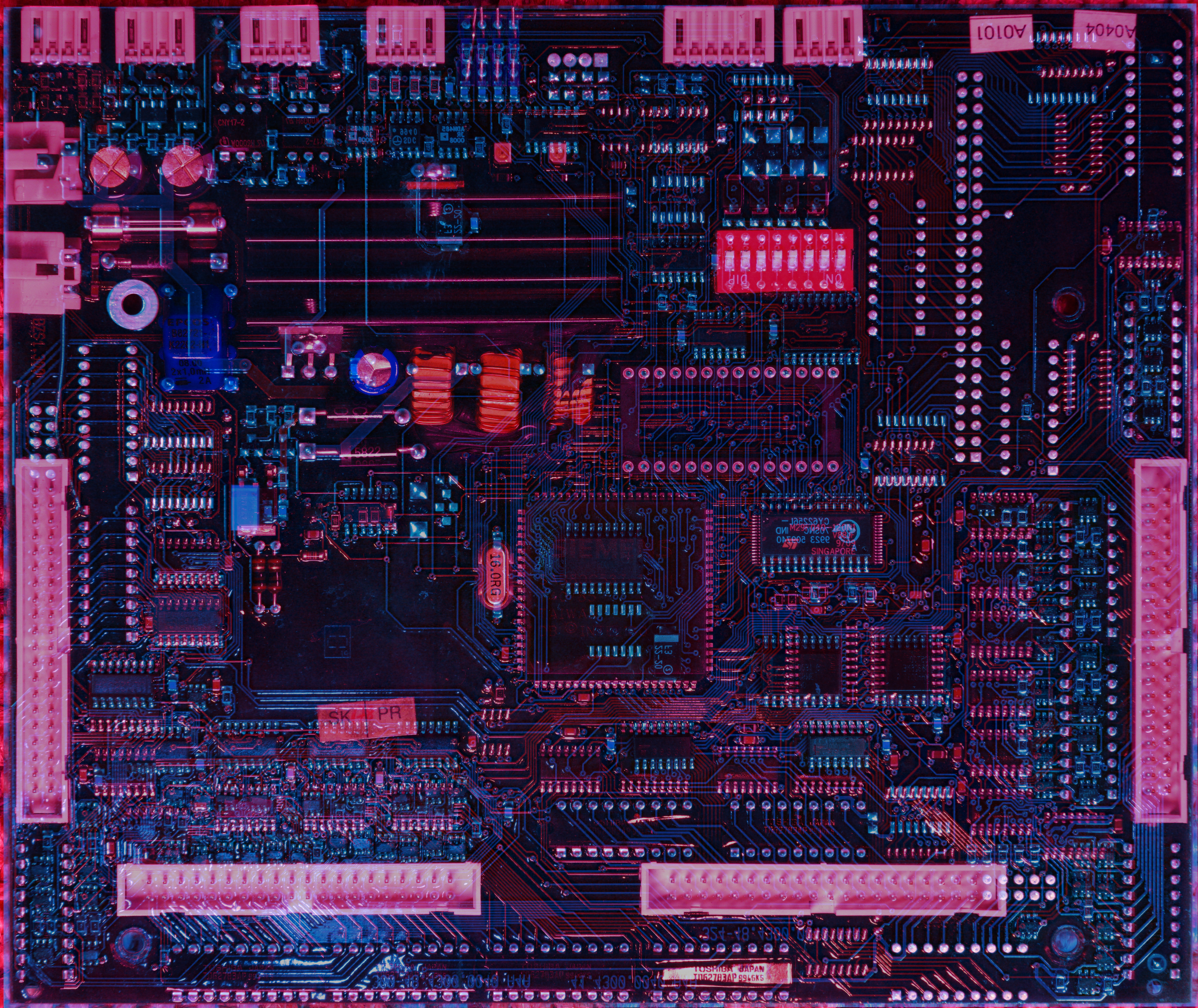
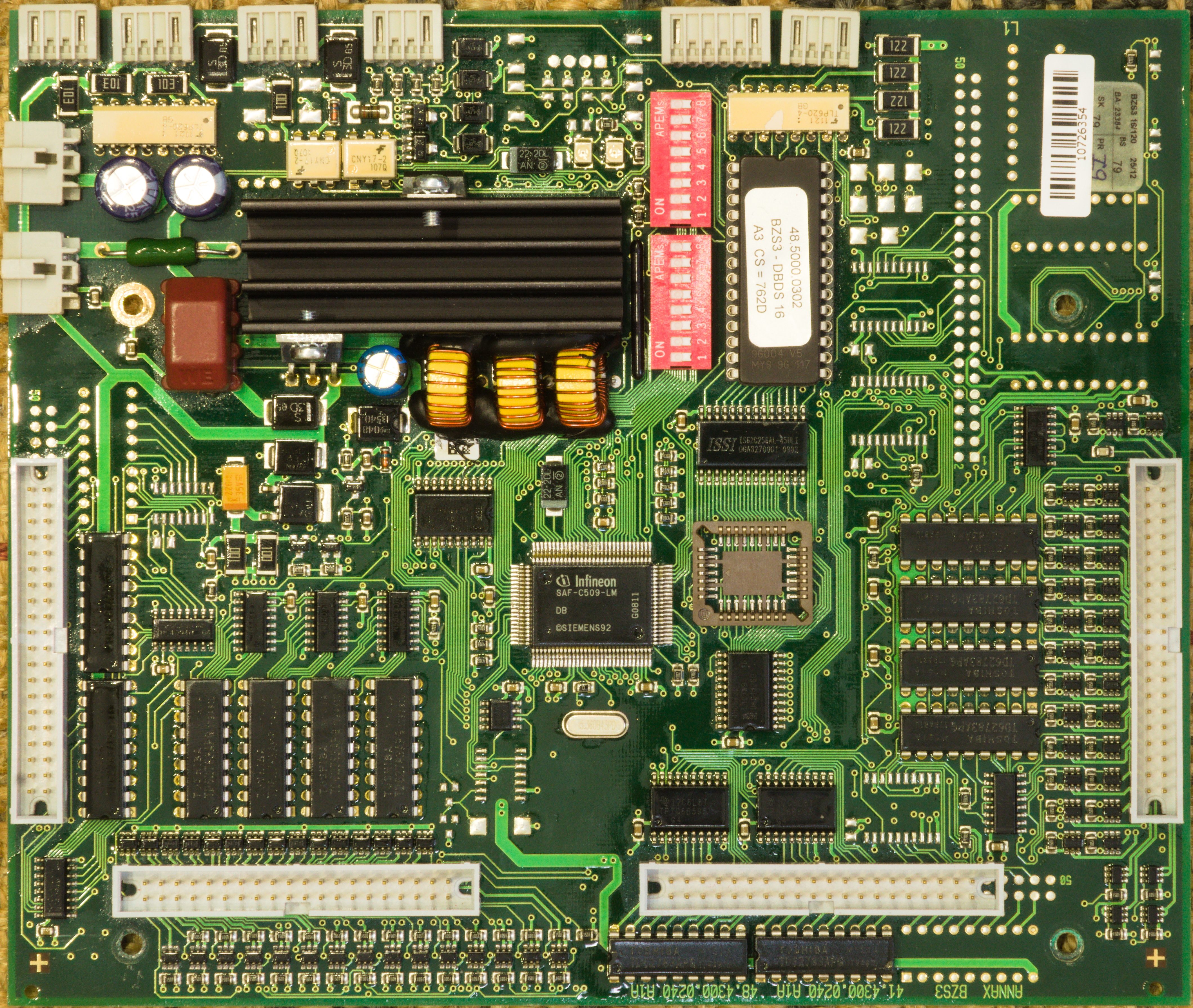
The control board (BZS3) is, at first glance, surprisingly simple for such a large display controller, and overwhelming at the same time.
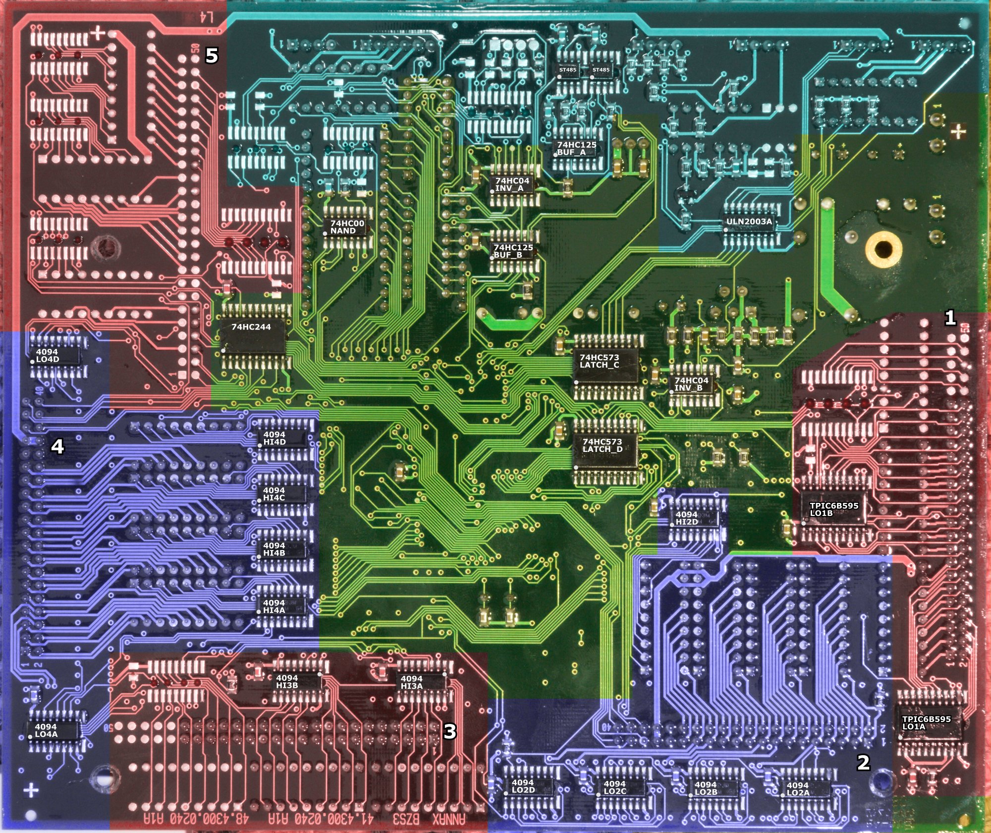
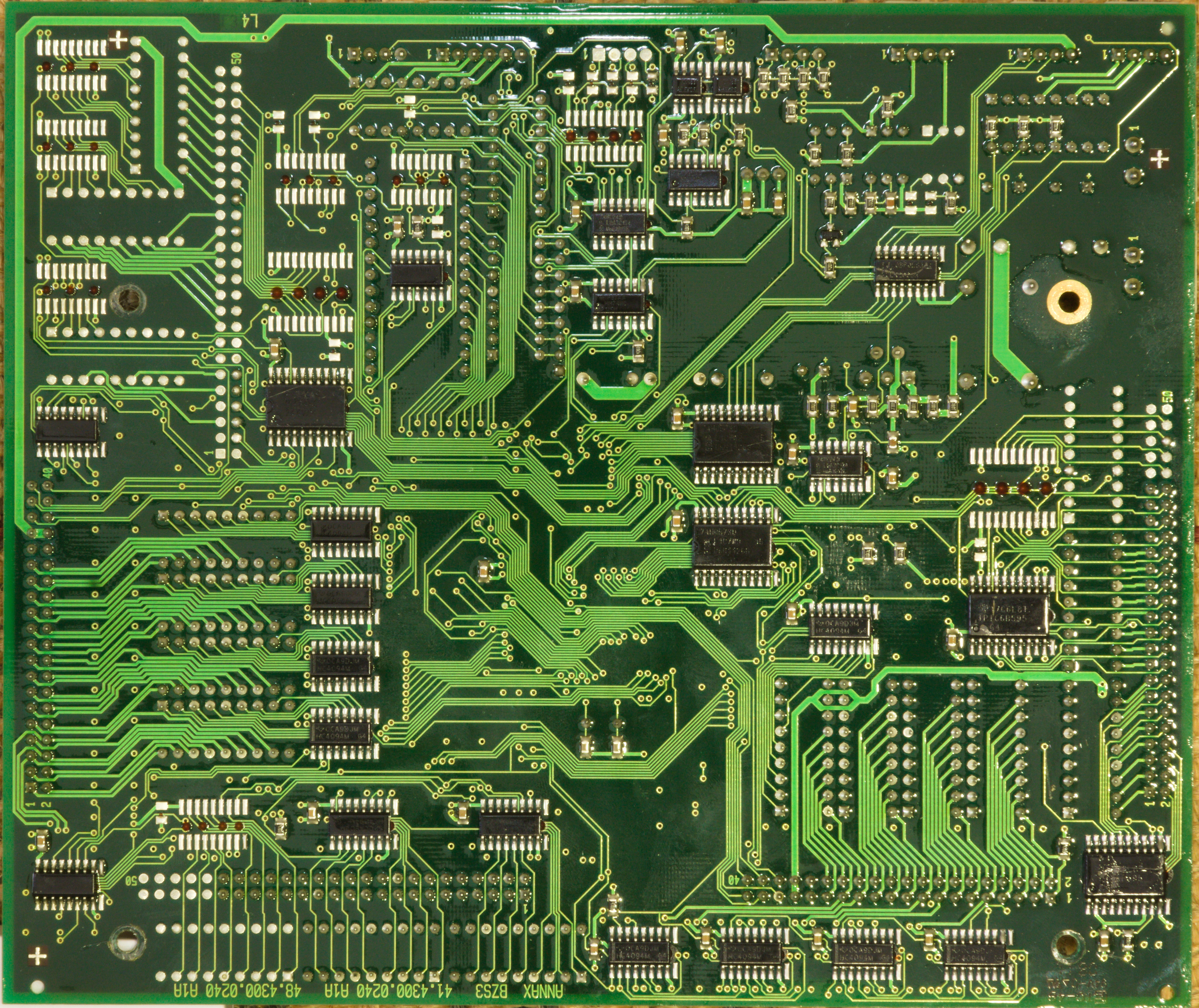
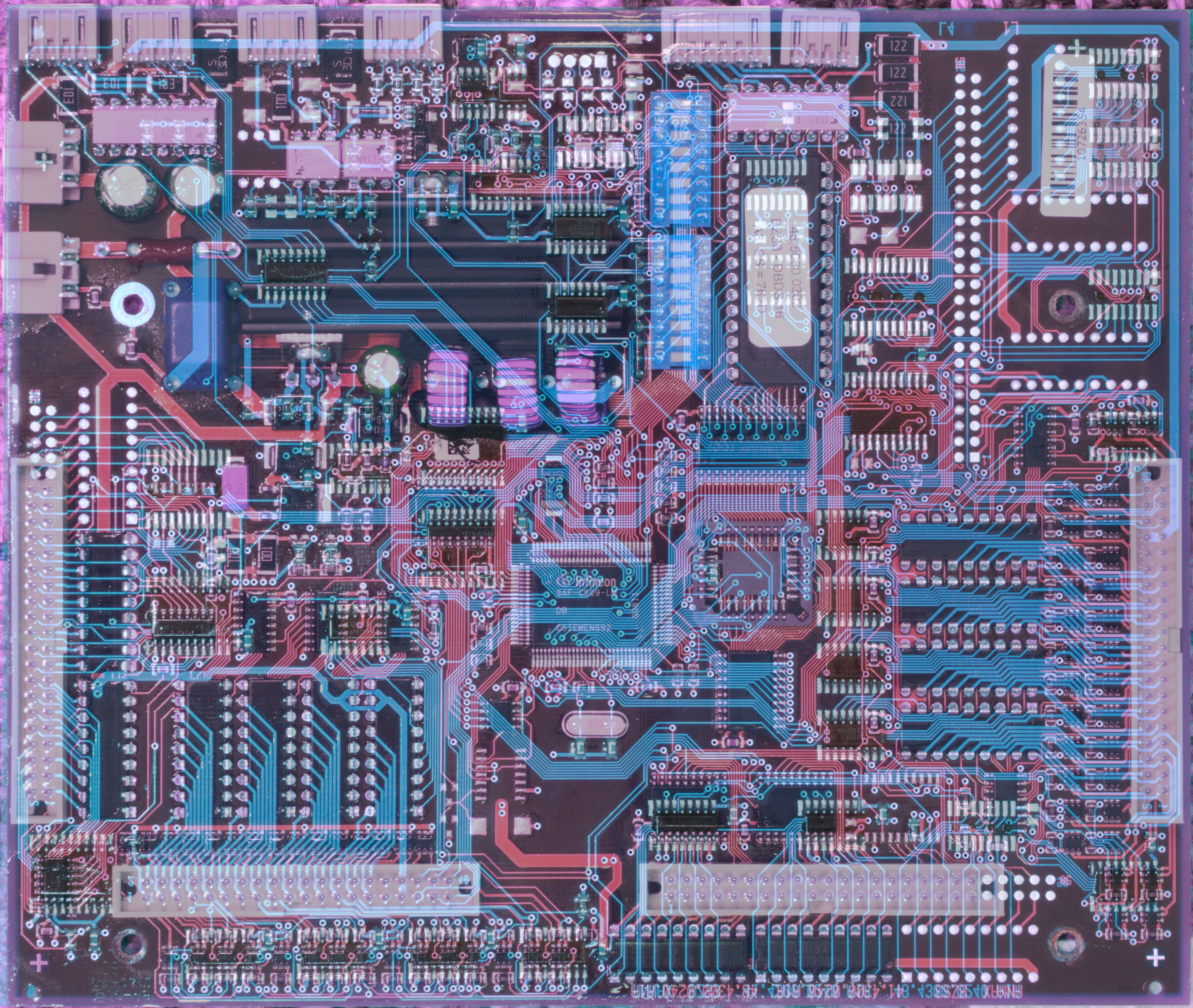
The two images on the right have most of their ICs labeled (model and an identifier, pin 1 designated with a white circle), and show the components, grouped and highlighted by their purpose. (You can also download the original high-resolution photos of the front, the back (The SOIC footprints on the bottom have unused pads to their right – these are "solder thieves", something that is useful for wave soldering. Keep this in mind, especially when looking at the empty footprints!), and both sides overlaid and aligned where front is red and back is blue.)
As the EPROM is socketed, it is quite easy to remove it and dump its contents for disassembly – something I'll do in a later part of this series.
The hardware supports display panels with up to 30 columns (two outputs of the last shift register are not connected) and up to 24 rows (if a third row shift register and driver would be installed, which is not the case in this board).
With the multiple row and column connectors, it becomes possible to control a maximum of 6 panels, as follows:
The firmware supports the full maximum of 180 × 24 pixels regardless of the driver ICs being installed or not, making this board suitable for various display sizes.
Naturally, each group of shift registers (such as "the ones for the 30 high-side drivers on column connector 2") forms a chain where the MCU talks to the first shift register and fills the others by pushing sufficiently many bits into it. The connectors (1-5) are all fed separately (from separate data lines on the MCU/the latches), however, the low and high sides are fed from the same data line. That is, the low- and high-side registers of one particular connector always store the same data. The output enable (The low side drivers of row 1/3/5 connectors use TPIC6B595, which use output disable (nOE) pins instead of output enable. For simplicity, I will refer to all of them as output-enable pins.) pins are used to determine whether the low- or high-side drivers are activated. Of course, at most one of the output-enable pins on each connector may be asserted at any given time, otherwise you get a short.
While the MCU can control the data lines of the shift registers on each connector individually, the clock and strobe signals of all rows are shared, and so are the signals for the columns. This means that pushing data into the connector 3 registers destroys the data in the connector 1 registers (unless you feed data into both data 1 and 3 pins at the same time). Typically this doesn't matter, as the data in the other registers are probably stale anyway by the time you want to activate them again (e.g. its current state is "row 16 only" but you'd want to start at row 1 anyway). For the flipdots alone, the data lines could have been merged (and panel selection be done exclusively with the output enable signals) and thus three pins could have been saved. However, this would not have reduced the required number of latches.
The C509 has many IO pins, but still not enough for all these control signals, which is why they're on three latches used as port extenders. The pin mapping is given below. The naming scheme as follows: HI-X_OE and LO-X_OE are output enable signals for the high- and low-side drivers of connector X respectively. The TPIC6B595 use inverted logic, so they use output disable signals, denoted as nOE below. DATA, CLOCK, STROBE are simply the signals of the corresponding shift register groups as described above.
Latch C has a few unrelated signals: the red status LED near the top of the board, and three open-collector outputs that are routed to the second connector at the top board edge. This particular display did not have these connected, though, and while the firmware contains functions to control these pins, they are never called, so I have no concrete idea what they were used for.
Separate from the shift registers described above, which control the flipdots, there are additional shift registers for the LED row signals (the flipdot low-side column drivers are re-used here). As written above, these registers are not on the main control board, but on each individual panel (probably because the connector layout evolved from a previous board without LED support, and there were not enough unused pins for all the LEDs). The control signals for these shift registers are placed on a few unused pins on the column connector. With individual shift registers for each panel, it is, in principle, possible to control all boards separately in parallel – and the firmware actually does that! I will describe this in a later part of the series.
Other than that, the LED shift registers are conceptually identical to the flipdot shift registers.
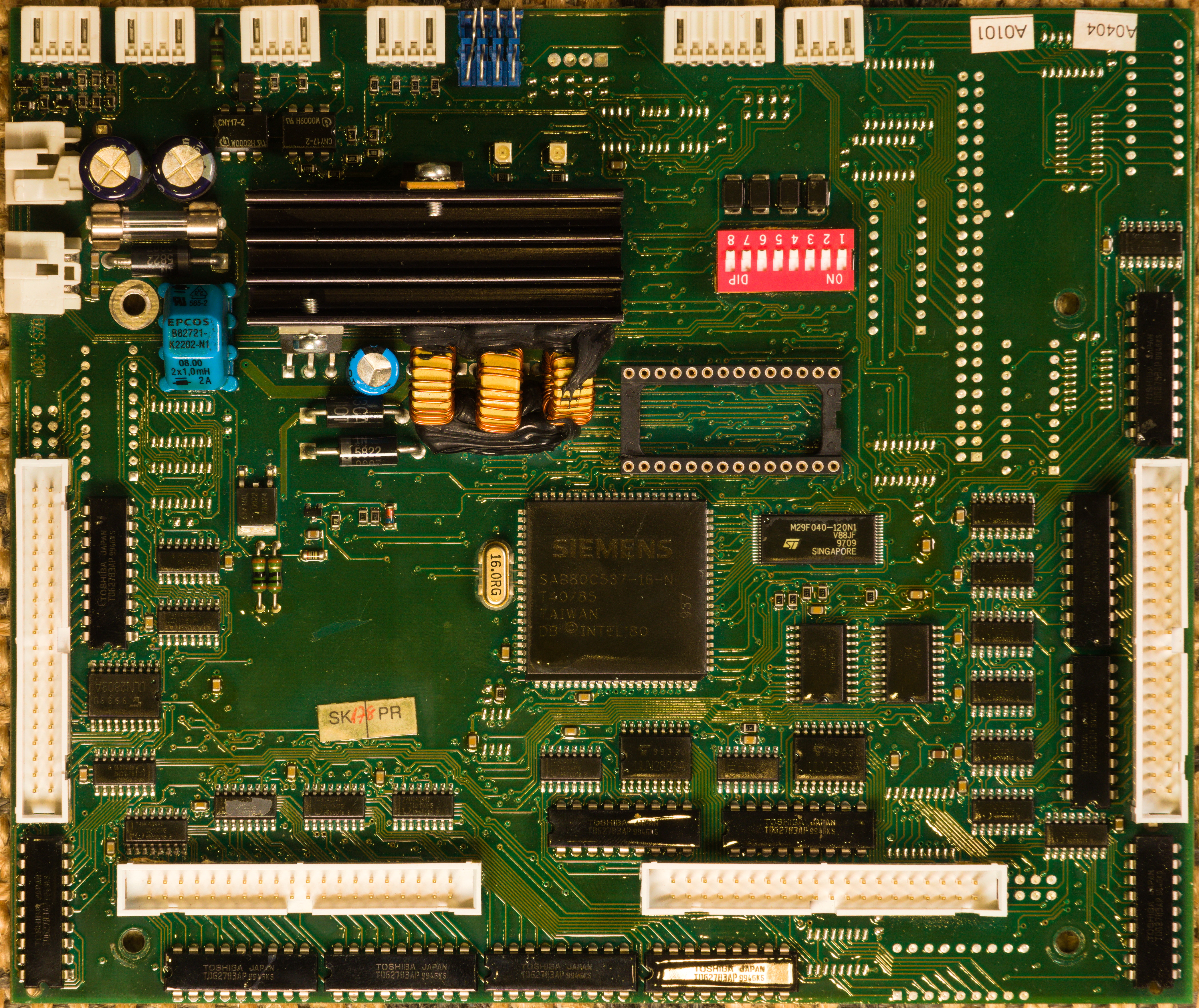
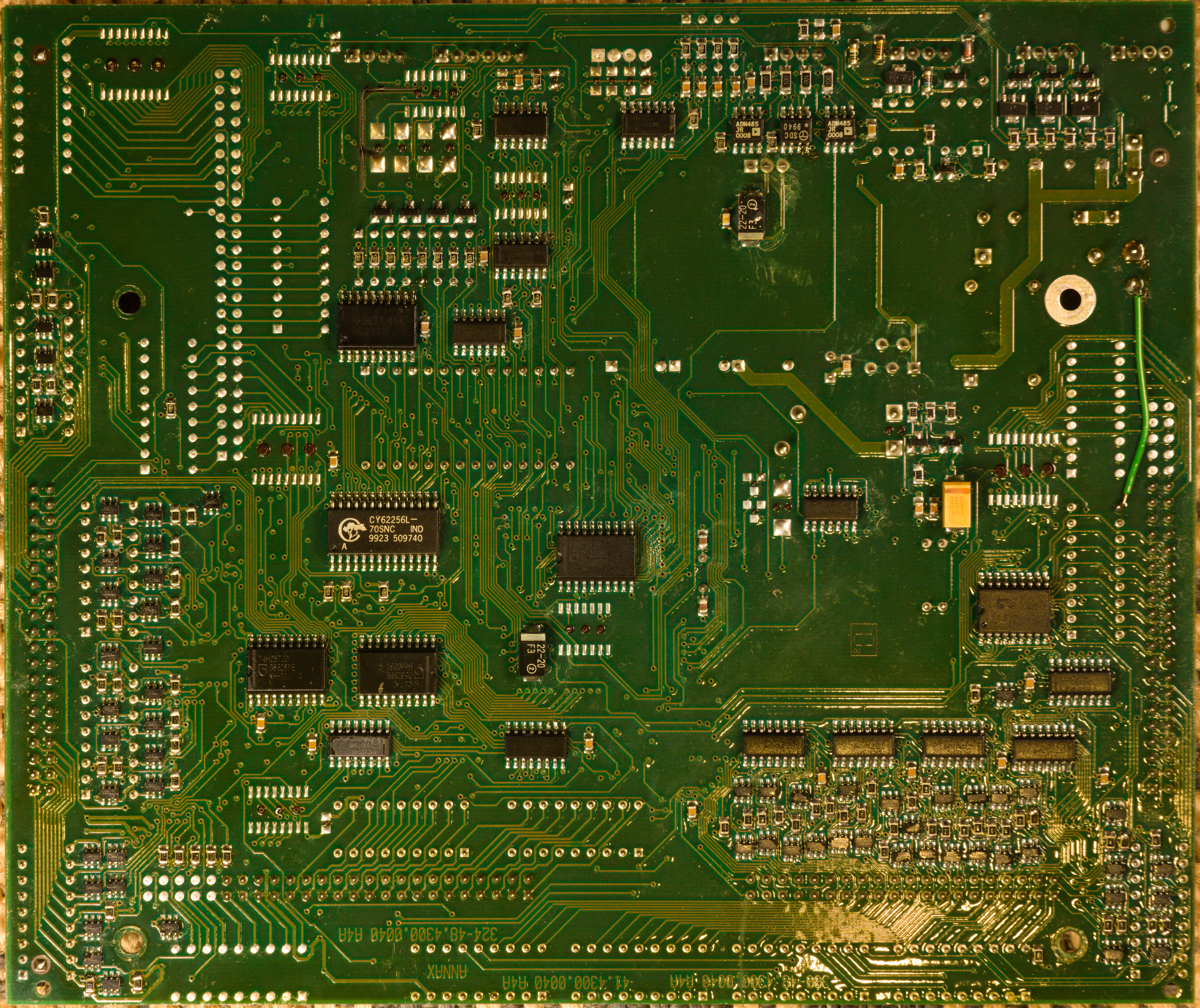
From a second display, I got a different, older version (BZS1) of the control board. Everything looks a bit more bulky and dated (older and larger SAB-80C537-16-N instead of the newer and more compact C509), and some components were sourced differently (such as SRAM). Instead of TPIC6B595 as low-side drivers, the more traditional combination of 4094+ULN2803A was used. The older version used a cartridge fuse instead of the pico-fuse (right next to the power connector) on the newer board. However, all the connectors are placed identically and it uses basically the same logic ICs (a bunch of 74HC573 used as I/O extenders, some 74HC00, 74HC04, 74HC125, 74HC244), just arranged slightly differently.
A quick glance at the firmware shows that it has the same structure, with most differences resulting from a different I/O port layout. Likely, boards BZS1 and BZS3 were supposed to be just a hardware revision, and to be used interchangeably as needed.
That's it for the first part of the series! In the following parts, we will discuss some parts of the control board in more detail, and have a look at the firmware.